pn junction diagram
Pn Junction With Diagram. 11 Pics about Pn Junction With Diagram : PN-Junction — Modern Lab Experiments documentation, PN Junction Theory - Electronics-Lab.com and also pn junction - In band diagram, why the Fermi energy (EF) is constant.
Pn Junction With Diagram
 ana-guterres.blogspot.com
biased reverse
PN-Junction — Modern Lab Experiments Documentation
 wanda.fiu.edu
junction pn diagram energy silicon type state band electric semiconductor current quantum diode between location difference materials modern scheme field
What Is A PN Junction Diode? - Polytechnic Hub
 www.polytechnichub.com
pn junction diode construction
PN Junction Theory - Electronics-Lab.com
 www.electronics-lab.com
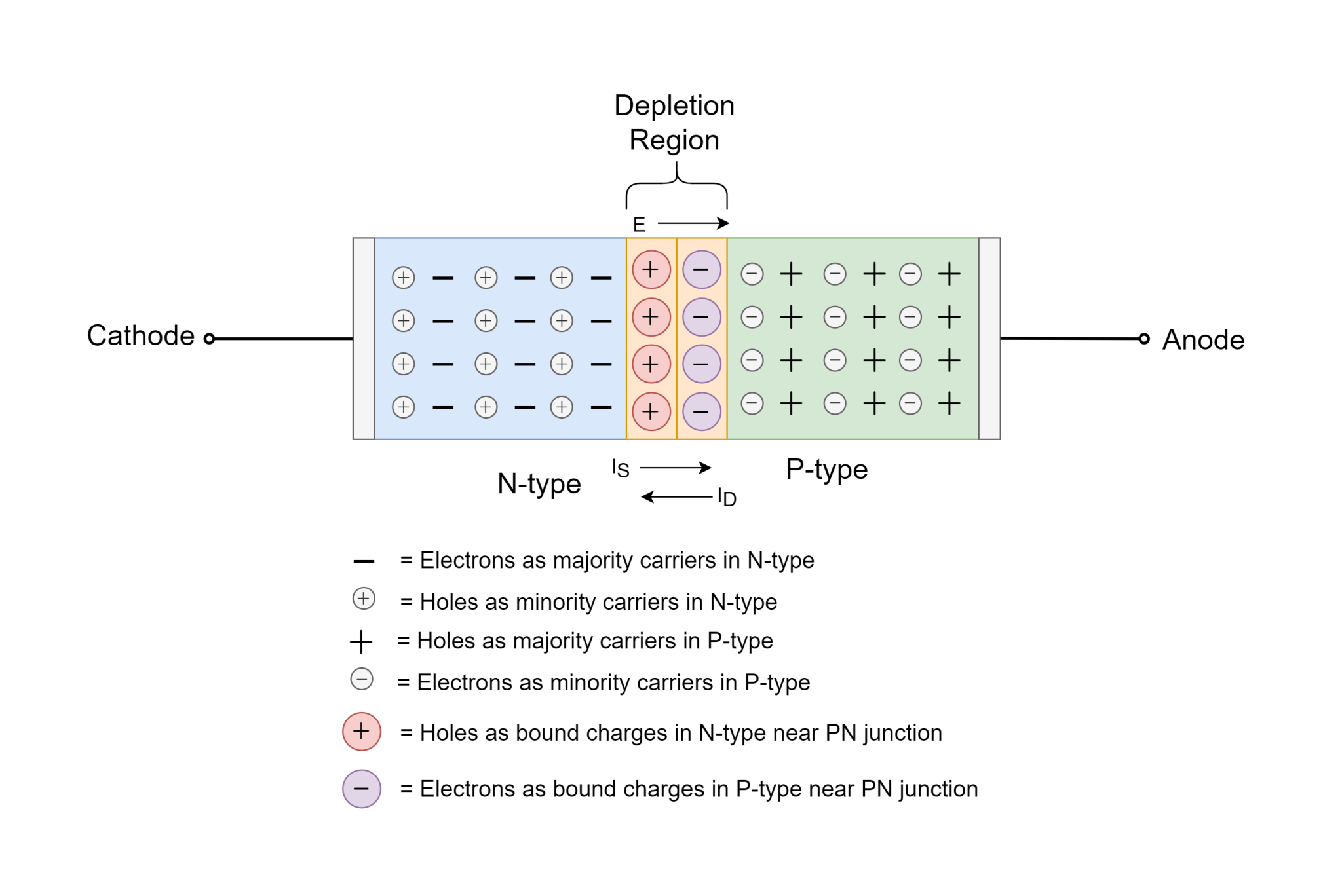
junction charges terminal
PN Junction Diode Theory - 2 Types Forward And Reverse Bias
 physicswave.com
junction diode theory
DIode Action
 www.michaelsharris.com
diode mechanism bias reverse forward working electronics characteristic current increase
Reverse And Forward Biased PN Junction & Fermi Level - Theory, Law Of
 www.youtube.com
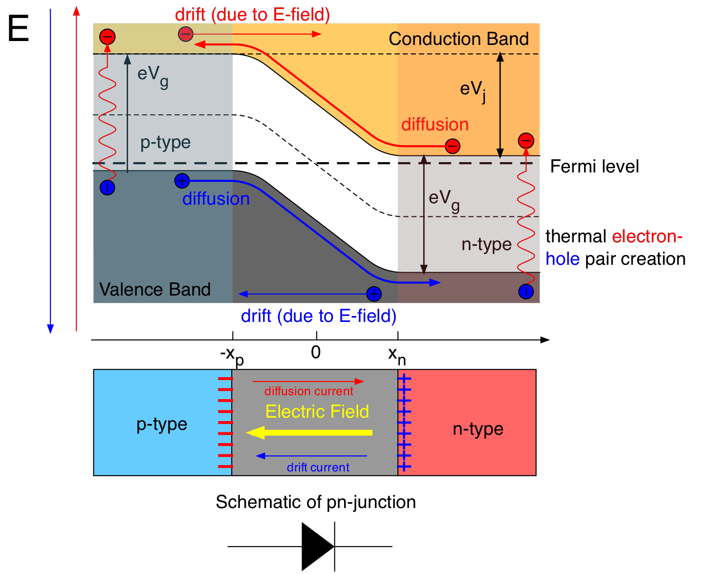
junction fermi band pn level reverse forward diagrams biased law
Pn Junction - In Band Diagram, Why The Fermi Energy (EF) Is Constant
 electronics.stackexchange.com
diagram band fermi energy ef pn device why junction level diagrams constant along source questions junctions stack
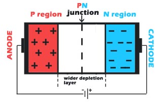
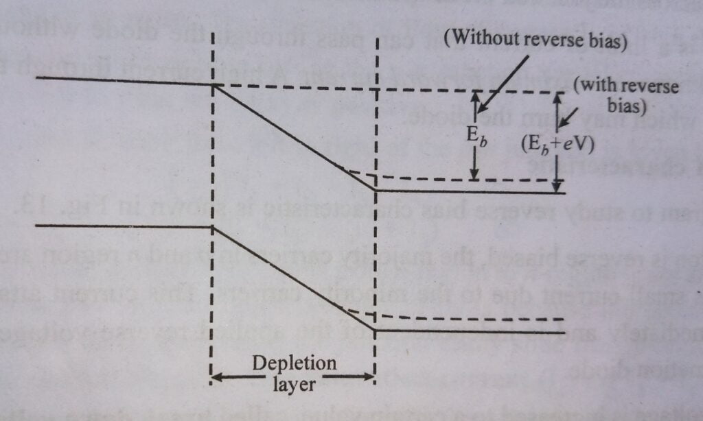
How Is A Depletion Region Formed? - Quora
depletion region formed semiconductors junction hyperphysics semiconductor negative positive electronics form quora
PN Junction Diode Theory - 2 Types Forward And Reverse Bias
 physicswave.com
diode bias
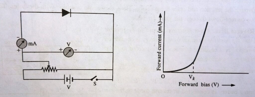
CBSE Biology Practical Class XII - Drawing I-V Characteristics Graph Of
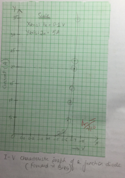 notesforfree.com
diode junction graph characteristics forward resistance state observation dynamic class iv table biasing drawing practical
How is a depletion region formed?. Pn-junction — modern lab experiments documentation. Pn junction with diagram