simplified band diagram electric field
(a) Unit cell of the bilayered chiral metasurface. (b) The photography. 11 Images about (a) Unit cell of the bilayered chiral metasurface. (b) The photography : (a) Schematic diagram of the energy band structure, plasmonic resonance, (a) Simplified cross-sectional view of a planar SOI n+/p−/p+ test and also IF-21.4 | 21.4 MHz IF amplifier module for FM receivers | Buy on-line.
(a) Unit Cell Of The Bilayered Chiral Metasurface. (b) The Photography
 www.researchgate.net
chiral metasurface bilayered polarization xiaodong metamaterial rotator
(a) Simplified Cross-sectional View Of A Planar SOI N+/p−/p+ Test
 www.researchgate.net
planar diode
Device Configuration And Experimental Set-up For MoS2 Valleytronic
 www.researchgate.net
mos2
(PDF) Charge Injection And Accumulation In Organic Light-emitting Diode
 www.researchgate.net
pss pedot emitting anode diode accumulation temporal intensity simplified voltages
Simplified Cross Section Of Zero-thickness CPW With Multilayer
 www.researchgate.net
cmos substrates waveguides characterization coplanar dielectric multilayer simplified
Cross Section Vs. Effective LET Graph For Two Circuits [14]. | Download
![Cross section vs. Effective LET graph for two circuits [14]. | Download](https://www.researchgate.net/profile/Ronald_Schrimpf/publication/3151317/figure/fig12/AS:668383867596801@1536366540158/Energy-band-diagram-comparison-of-a-Si-BJT-solid-line-and-SiGe-HBT-dashed-line-biased_Q320.jpg) www.researchgate.net
www.researchgate.net
sige bjt hbt biased dashed
Nazmul AHSAN | Associate Professor (Research) | Doctor Of Engineering
 www.researchgate.net
Expected Values Of The Spin Operator For The Band Structure Of A Na3Bi
 www.researchgate.net
IF-21.4 | 21.4 MHz IF Amplifier Module For FM Receivers | Buy On-line
 www.rf-microwave.com
module amplifier mhz receivers fm microwave rf diagram simplified electrical
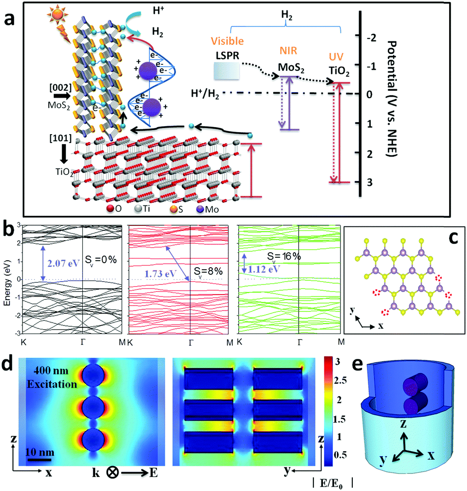
MoS 2 /TiO 2 Heterostructures As Nonmetal Plasmonic Photocatalysts For
 pubs.rsc.org
photocatalysts plasmonic mos rsc structure nonmetal tio efficient hydrogen heterostructures highly evolution
(a) Schematic Diagram Of The Energy Band Structure, Plasmonic Resonance
 www.researchgate.net
plasmonic structure schematic dft electron heterojunction
(a) schematic diagram of the energy band structure, plasmonic resonance. Simplified cross section of zero-thickness cpw with multilayer. Cmos substrates waveguides characterization coplanar dielectric multilayer simplified